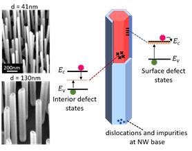
Our team’s goal is to use NWs to develop novel semiconductor optoelectronics devices, such as, photovoltaics, lasers, and LEDs. We are developing the selective area epitaxy (SAE) technique to grow III-V NWs on inexpensive silicon substrates utilizing molecular beam epitaxy. The NW carrier dynamics and optoelectronic response are characterized by ultrafast optical pump-probe spectroscopy, quantum efficiency, and photoluminescence measurements.
Collaborator on the project includes Professor John Prineas' lab at UIowa. Funded by the National Science Foundation Electronics, Photonics and Magnetic Devices (EPMD) program.